Paragraf Redefines Medical Diagnostics with Graphene-Based Biosensors Capable of Detecting Diseases in Minutes

Paragraf
Graphene Device Manufacturer
“The 19th century was the age of iron, the 20th century was the age of silicon, and the 21st century is the age of carbon.” This statement gained popularity in the materials industry a decade ago, and it remains relevant today. Whether it is an exaggeration may only be determined decades from now. However, since British physicists A. Geim, K. Novoselov, and others first isolated graphene from graphite in 2004, companies worldwide have flocked to the graphene industry. Among them, the startup Paragraf has leveraged its unique patented technology to bring innovative advancements to graphene applications.
Paragraf is a technology company that produces high-quality, large-area graphene electronic devices.。Recently, the company successfully completed a $60 million (£45 million) Series B financing round., this financing round was led by New Science Ventures, with participation from existing investors including In-Q-Tel, Parkwalk Advisors, Molten Ventures, and IQ Capital.This round of financing will be used to expand business scale, enhance R&D capabilities and infrastructure, with the goal of enabling Paragraf to further expand, particularly into international markets.
Headquartered in Somersham, Cambridgeshire, UK, Paragraf is a supplier of graphene-based electronic devices that spun out from the Department of Materials Science at the University of Cambridge. It was co-founded in 2015 by Professor Simon Thomas and Dr. Colin Humphreys.
Simon Thomas, the company’s CEO and founder, has a multidisciplinary background in physics, engineering, and materials science, enabling him to truly grasp cutting-edge graphene production technologies and apply them to existing products.
Another co-founder, Colin Humphreys, has a proven track record of commercializing cutting-edge science, having established multiple technology companies spun out from prestigious universities. For instance, he guided the creation of the Rolls-Royce University Research Centre, which is currently supplying novel alloys for Rolls-Royce aero-engines.
Not only the two founders, but also Paragraf’s executive team have backgrounds in materials science., laying the foundation for Paragraf to remain at the forefront of the graphene field.
Core Patent: Direct Deposition of Graphene on Semiconductor-Compatible Substrates
Graphene is a two-dimensional material composed of a single layer of carbon atoms, in which the atoms are interconnected via sp² hybridization to form hexagonal ring structures, thereby creating a honeycomb-like lattice. This characteristic enables graphene to provide more biorecognition sites per unit area than other materials. Furthermore, electrons migrate through graphene at an extremely high velocity—reaching 1/300 of the speed of light—which endows graphene with excellent electrical conductivity. These properties collectively facilitate the application of graphene in the field of biosensing, enhancing key performance metrics of biosensors such as sensitivity and integration capability.
Because graphene consists of a single layer of carbon atoms, it is extremely thin. This makes small-scale laboratory preparation relatively easy, but large-scale industrial production remains challenging.
Currently, the most commonly used method for industrial-scale graphene production is chemical vapor deposition (CVD). In the CVD process, metals such as nickel (Ni) and copper (Cu) serve as growth substrates. A carbon-containing precursor is introduced as the carbon source; under high temperatures, the precursor decomposes to release carbon atoms that deposit onto the metal substrate, forming a stable graphene film.
However, graphene prepared via the traditional chemical vapor deposition (CVD) method is attached to a metal substrate and cannot be directly applied in sensors. It requires etching away the original metal substrate and transferring the graphene onto a semiconductor-compatible substrate. This process inevitably induces graphene wrinkling and may cause contamination. Such wrinkles and contamination lead to structural incompleteness, which significantly degrades the performance of the graphene.
Paragraf pioneered and patented a technology for producing graphene using Metal Organic Chemical Vapour Deposition (MOCVD).
MOCVD is a term in the field of manufacturing processes, used to describe a class of techniques for directly depositing ultra-thin single-crystal layers on semiconductor wafers. This technique has significantly higher requirements for temperature control and raw materials compared to the CVD method.Paragraf is the first manufacturer to apply the MOCVD method to the mass production of graphene. Although previous patents have described the use of MOCVD for graphene production, none of them reported production outcomes.
According to the patent description obtained by Paragraf, their production process is divided into two parts.
Part I: High-Temperature Synthesis of Graphene, first load the semiconductor substrate (e.g., silicon, gallium nitride, silicon carbide, or silicon-germanium) into the MOCVD reaction chamber, and then introduce an organic compound containing at least one heteroatom, mixed with a diluent gas, into the reaction chamber. (Organic compounds refer to compounds that contain carbon and typically possess at least one covalent bond, such as C–H or C–C bonds; heteroatoms refer to atoms other than carbon or hydrogen. The heteroatoms in the organic compounds selected for this process are preferably metal atoms, or nitrogen, sulfur, phosphorus, silicon, or halogens.)
Paragraf found that when trimethylgallium Ga(CH3)3 is used as a precursor, the resulting graphene does not contain Ga doping; therefore, this process can utilize lower-cost heteroatom-containing organic compounds.
After introducing the precursors, the reaction chamber temperature is raised to 1050°C and the substrate temperature to 1350°C, at which point the carbon fully decomposes. A substantial and uniform flow of raw materials must be maintained during this step to ensure uniform deposition of graphene on the substrate.
Part 2: Depositing Graphene onto a Semiconductor Substrate: Within 15 minutes after the complete decomposition of carbon, cool the reactor to room temperature and allow the pressure to return to atmospheric pressure, with graphene deposited on the semiconductor substrate. The challenge in this step lies in precise temperature control; most current MOCVD methods employ isothermal processes, making it difficult to achieve uniform cooling, which adversely affects the graphene structure.
Paragraf has developed a technology that enables the direct growth of graphene on semiconductor substrates, eliminating the need for transfer processes and saving time. This approach avoids the consumption of copper metal substrates and etching solutions, thereby preventing the generation of waste liquids that could pollute the environment. Most importantly, the resulting graphene exhibits high structural integrity, ensuring superior performance in graphene-based electronic devices.
At the end of 2021, Paragraf was shortlisted for the UK TechWorks Electronics Technology Innovation Award with this proprietary technology.
Graphene Hall Effect Sensors: Delivering Ultra-High Performance in Extreme Environments
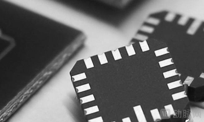
Leveraging MOCVD as its core technology, Paragraf has launched three flagship products: Hall effect sensors, biosensors, and solid-state devices.
Paragraf’s GHS series of Hall effect sensors comprises two products: GHS-A and GHS-C.
 Product Image Source: Paragraf Official Website
GHS-A is recommended for use at room temperature,to achieve optimal performance, although it also performs well in lower-temperature environments, making it suitable for applications such as electric vehicles, local current density analysis, and batteries.
GHS-C is suitable for ultra-low temperature environments, designed for ultra-high-resolution magnetic field measurements across extreme temperature and magnetic field ranges. As a two-dimensional nanomaterial, graphene is highly sensitive to ambient temperature fluctuations, which makes graphene-based sensors, despite their robust performance, susceptible to thermal interference. According to Paragraf, the GHS-C achieves a resolution of <0.2 ppm, operates at picowatt-level power consumption, and can withstand temperatures as low as -271 °C (1.8 K). The GHS series has successfully met the challenges posed by extreme temperature conditions for sensors.
Moreover, conventional magnetic field sensors on the market are all subject to planar Hall effect interference with measurement results, and research by the European Organization for Nuclear Research (CERN) has found thatParagraf's graphene Hall-effect sensors exhibit virtually no planar Hall effect during operation., therefore this product can also be used in local magnetic fields.
In 2020, Paragraf’s GHS series sensors entered the market., initially supplying products in small batches before gradually expanding its market presence. Currently, Paragraf’s graphene Hall-effect sensor GHS series is widely used in aerospace, semiconductors, healthcare, automotive, scientific research, industrial, and quantum computing applications.
Paragraf hopes that its graphene Hall-effect sensors will become the standard battery components for next-generation battery systems.
Graphene Biosensors: Aiming to Transform Healthcare with Instant and Accurate Detection
Paragraf’s first core product, the GHS series, has been widely adopted since its market launch, and its next breakthrough productGraphene Biosensors – The GBS Series is Under Development。
According to Paragraf, the GBS series can complete testing for several common diseases within minutes, accelerating diagnostic throughput at primary care hospitals and enabling more timely and precise treatment plans for patients. The product is expected to be applied in fields such as clinical medicine, veterinary medicine, environmental monitoring, agriculture, and food safety.
Paragraf believes that although the two widely used detection technologies—immunoassays and nucleic acid amplification techniques (such as PCR)—are technically mature, they still have limitations in practical applications. First, sample preparation for both technologies is complex, requiring sophisticated laboratory equipment and close coordination with skilled operators; second, these two technologies are incompatible and cannot be performed simultaneously on the same device. Due to these two constraints, primary healthcare institutions are often unable to conduct accurate and immediate disease diagnoses.
The Paragraf Graphene Biosensor (GBS) series has the potential to enable accurate point-of-care diagnostics.
Good Biocompatibility of Graphene, enabling biomolecules such as nucleic acids, proteins, glucose, peptides, and microorganisms to be attached to the graphene surface via physical adsorption or chemical bond conjugation, which means that graphene can simultaneously detect multiple types of biomolecules.
Graphene also exhibits extremely high electron mobility., laying the foundation for high-speed and sensitive biosensing. The combination of excellent biocompatibility and high sensitivity enables the GBS series to detect pathogens at extremely low concentrations in fluids and gases.
Meanwhile, the working mechanism of graphene biosensors is to convert biological signals into electrical signals, allowing tests to be completed in an instant, thus eliminating the need for complex sample preparation required for optical detection.
Paragraf has achieved a reproducible graphene manufacturing process, ensuring that each batch of material is identical in size and quality. This consistency guarantees quantitative accuracy in every measurement, allowing multiple tests to be performed using only a small-volume sample from the patient.
To further enhance the patient experience, Paragraf is collaborating with experts in the field of public and patient involvement (PPI) to incorporate perspectives from patients and the public into the research and development of graphene biosensors, thereby addressing broader societal needs.
In January this year, Paragraf appointed Malcolm Stewart as Director of Business Development for its graphene biosensor product line. With extensive knowledge and experience in the biomedical field, Mr. Stewart is expected to foster collaborations with industry experts upon joining, further advance graphene production technologies, and leverage his solid and broad biomedical expertise to shorten R&D cycles. This move offers a glimpse into Paragraf’s commitment to the research and development of graphene-based biosensors.
Regarding the commercial vision for graphene biosensors, Paragraf has stated outright that its goal is to market its GBS series of biosensors globally. Currently, Paragraf is seeking established medical device suppliers with whom it can collaborate.
In addition to biosensors, Paragraf is also developing the GSS series of graphene solid-state devices., such as transistors and optical modulators. However, the GSS series appears to have a longer road ahead compared to the former.
Outsource packaging and assembly tasks to ensure core business operations
Technological advancements can truly benefit society only when they move beyond the laboratory. Paragraf is dedicated to this very mission: commercializing cutting-edge technologies. However, as a single company, Paragraf cannot currently handle all stages from graphene production to material encapsulation and component assembly. Therefore, it collaborates with wafer foundries to ensure it can focus its efforts on researching and developing graphene production.
In the course of collaborating with wafer foundries, Paragraf identified a new challenge: although manufacturers were interested in graphene, they remained concerned that the use of this novel material might contaminate their production lines. To allay these concerns, Paragraf conducted pilot runs on three independent production lines, demonstrating that its products are compatible with existing manufacturing processes.
Paragraf deeply understands that success requires collaboration. The company engages in extensive partnerships not only in product manufacturing but also in graphene research and development. It has collaborated with many globally renowned organizations, including the European Organization for Nuclear Research (CERN), the National Physical Laboratory, and Rolls-Royce, covering fields such as sensor and semiconductor technologies.
Thomas, co-founder and CEO of Paragraf, said: “Our goal is to continuously enhance the performance of electronic devices and steadily reduce humanity’s reliance on electricity. Graphene-based electronics are still in their early stages, with a long road ahead, but we can already see their future.”
China's Graphene Sector Sees Fierce Competition: A Resource Powerhouse with the Highest Total Number of Patents
Over the past decade, graphene has remained a hot topic in the field of materials science, regarded as the “future material of the 21st century.” Approximately 80 countries worldwide and tens of thousands of enterprises have entered the graphene industry, including U.S. tech giants IBM and Intel. As the “birthplace” of graphene, the United Kingdom has long maintained a leading position in research.
China is a major country in natural graphite resources, with its output accounting for nearly half of the world's total production. It holds inherent advantages in the graphene industry. China ranks first globally in the number of graphene-related patent applications. Currently, there are over 10,000 domestic enterprises involved in graphene production and application, most of which are small and medium-sized enterprises concentrated in the eastern coastal regions.
In China's graphene industry, leading enterprises include Fangda Carbon, BTR, Sixth Element, Tanyuan Technology, and Ningbo Moxi. The annual production capacity of graphene films by these companies can reach the million-square-meter level, with each company focusing on different business areas. For instance, Fangda Carbon mainly produces graphite electrodes, special graphite products, and raw materials for carbon product manufacturing; BTR manufactures artificial graphite anodes and natural graphite anodes; and Sixth Element primarily produces graphene powder materials.
It is evident that China’s graphene industry has a large number of existing competitors, resulting in intense competition within the sector. The upstream segment of the graphene industrial chain consists of graphite mine suppliers; due to the high degree of product homogenization, their bargaining power is relatively low. The midstream segment comprises graphene manufacturers. The downstream segment involves graphene-based application products, which are influenced by upstream graphene production capacity. Currently, these applications primarily span the fields of optoelectronic devices, energy technologies, and sensors.
Currently, the application of graphene in the field of biosensors is still in the research and development stage and has not yet achieved large-scale commercialization. It is far less mature than graphene sensors in other fields; however, with future improvements in policies and technology, graphene biosensors are expected to gradually mature.