HanHua Semiconductor Files IPO Prospectus: Pioneering Cross-Disciplinary Innovation in Microfluidic Chips for Life Sciences
The advent of semiconductor microfluidics technology is the result of humanity’s relentless pursuit of automation and high efficiency. As a foundational, cross-cutting technology, it facilitates the rapid development of interdisciplinary fields such as life sciences, biopharmaceuticals, and virtual and augmented reality.
Microfluidic chips are downstream application units of microfluidics technology. By leveraging Micro-Electro-Mechanical Systems (MEMS) technology, they enable the construction of miniaturized biochemical analysis systems on chip surfaces to rapidly and accurately process and detect proteins, nucleic acids, or specific targets. This approach consolidates key steps—such as sample preparation, biochemical reactions, and result detection, which traditionally require laboratory settings—onto a single tiny chip, earning them the industry acclaim of “Lab-on-a-Chip.”
As one of the current frontiers of technological innovation, semiconductor microfluidic chips are widely used in critical fields such as biomedical research, medical devices, drug synthesis and screening, food and commodity inspection, environmental monitoring, and aerospace science, owing to their high level of integration, rapid analysis, high efficiency, low energy consumption, and minimal pollution.
However, while technology brings convenience, microfluidics still faces certain pain points that urgently need to be addressed.
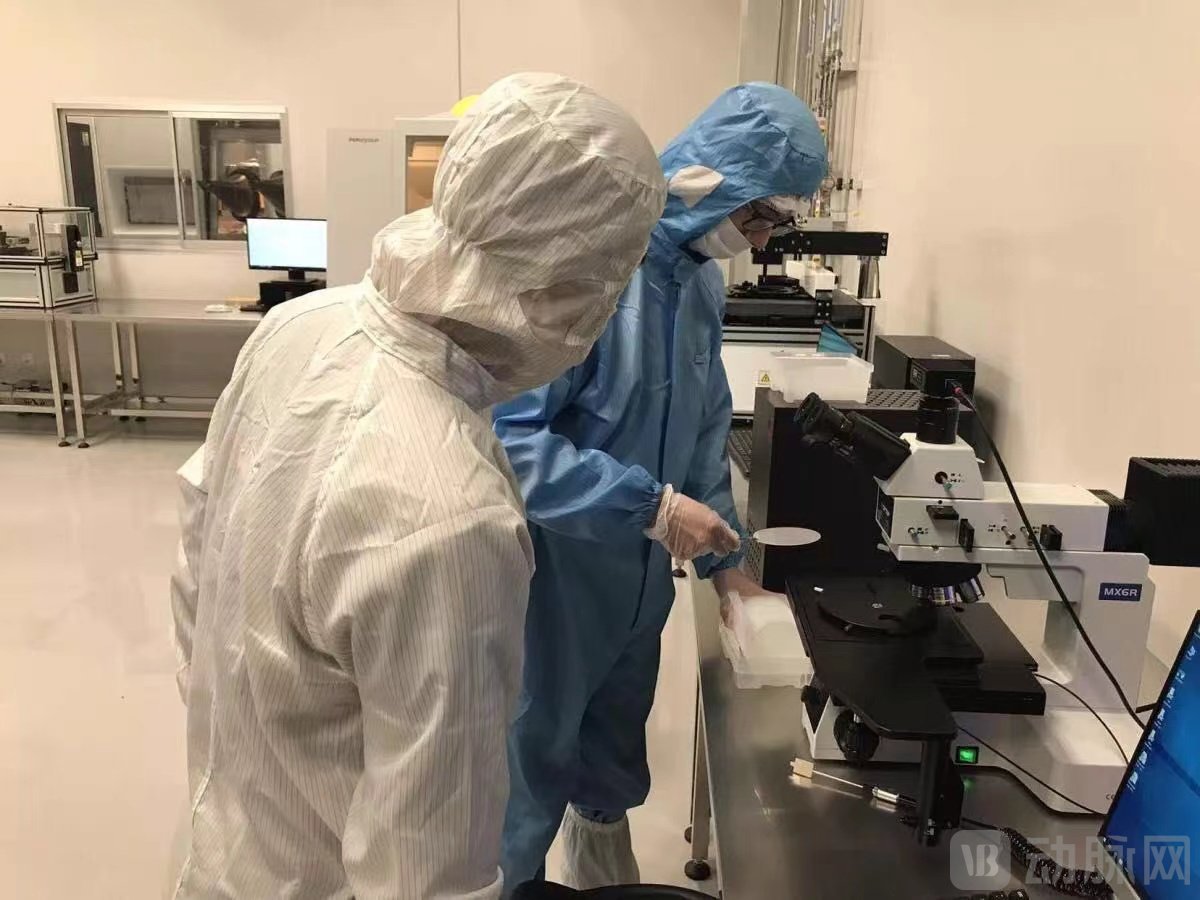
According toXu Wenjun, Assistant to the General Manager of HANHUAIntroduction. Currently, the pain points of microfluidic technology are mainly reflected in two aspects: first, how to design chips based on specific downstream application requirements and efficiently realize them through advanced semiconductor processes; second, the capability for mass production with large scale, high yield, and high throughput. As most microfluidic chips are applied in the life sciences and healthcare sector, which boasts broad prospects and a huge market size, the chips’Production Capacity RequirementsandCost ControlAll have set forth very high requirements.
HANHUA is a semiconductor materials and chip supplier integrating advanced R&D, large-scale manufacturing, testing, and technical services. It is dedicated to addressing critical challenges in the life sciences sector by leveraging advanced semiconductor materials and processes.
Leveraging HANHUA’s large-scale semiconductor production base, advanced semiconductor materials and chip processing technologies, a technically and managerially seasoned team with extensive mass-production experience, as well as a comprehensive production management and quality control system, the company is better positioned to deliver high-quality chip products to downstream customers on time and to specification, while also achieving tighter cost control.
In 2017, HANHUA was co-founded by overseas top-tier teams, with the Yangtze River Delta National Innovation Center/Jiangsu Industrial Technology Research Institute and Suzhou Industrial Park serving as its founding cornerstone partners. The core team members each possess over 10 years of experience in core R&D and production across the entire industry chain, ranging from materials to chip development.

Since its inception, HANHUA has pioneered room-temperature heterogeneous wafer hybrid bonding technology, achieving the hybrid integration of 8-inch CMOS with other heterogeneous semiconductor materials and chips (such as GaN full-color display chips).
This technology enables heterogeneous wafer integration of compound semiconductors with silicon-based CMOS, while employing the most advanced 3D IC hybrid wafer bonding technology to achieve high-density interconnection of electrodes for driver and functional circuits. This compatibility with large-scale integrated circuit manufacturing processes positions it as one of the most cutting-edge technologies in the semiconductor chip industry.
Ultra-High-Density MicroLED Micro-Display Chip Based on Hybrid Integration Technology: Development of Gallium Nitride (GaN) LED Arrays with Pixel Pitches Below 5 Micrometers, Addressing Key Challenges in Yield, Luminous Efficiency, and Crosstalk. Furthermore, by employing heterogeneous wafer bonding technology, the bottleneck of thermal expansion mismatch between nitride LED wafers and large-scale integrated circuit CMOS wafers is overcome, enabling the direct transfer of GaN MicroLED arrays onto CMOS driver array chips and achieving individual addressable illumination for each LED.
According to reports, this technology can be innovatively applied across disciplines in fields such as life sciences.Addressing challenges related to engineering, systematization, and high integration in the life sciences field。
Over the past decade, microfluidic technology has matured significantly in its applications within the biotechnology sector, including nucleic acid isolation and quantification in cell biology, DNA sequencing, analysis of gene mutations and differential gene expression, protein fractionation, drug research, and biomimetic studies.
As the functionality and integration level of microfluidic chips continue to improve, their fabrication processes are becoming increasingly complex, leading to a growing demand for integration with CMOS integrated circuits.This poses greater challenges to the precision and yield of chip fabrication processes.
“Cross-sector integration and cross-sector innovation are undoubtedly the future trends. We aim to leverage semiconductor materials and hybrid integration technologies as a bridge across disciplines, providing shared hard-tech solutions to address needs in life sciences and other interdisciplinary fields,” said Xu Wenjun.
According to Xu Wenjun, semiconductor microfluidic chips originally evolved from MEMS technology. By employing microfabrication processes, various microstructural units ranging from micrometers to sub-millimeters in size are fabricated on substrates made of different materials, thereby enabling fluid manipulation at the micrometer scale.
Currently, microfluidic chips on the market are mainly divided into two categories. One category consists of plastic chips fabricated using conventional micro-injection molding techniques. These chips primarily rely on external auxiliary equipment, such as fluid delivery tubing and detection modules, and are mainly suitable for traditional applications that do not require high precision or high levels of integration.
HANHUA’s microfluidic chip is built on silicon or other semiconductor materials, leveraging semiconductor technology to integrate a series of actuators and sensors—including processing circuits, liquid-driving MEMS structures, and liquid-phase detection electrodes—and achieves high-density integration directly with CMOS through 3DIC technology, thereby completely eliminating the need for external auxiliary equipment and enablingOn-Chip Integrated Microfluidic Systemsfunctionality. Its advantage lies in havingHigher precision and higher throughput significantly reduce testing time and improve accuracy, while revolutionarily enhancing integration.
In addition, HANHUA’s independent large-scale production line can rapidly achieve chipMass production, high yield rate, and controllable costs.
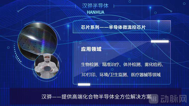
Currently, HANHUA has applied this chip to fields such as nebulized drug delivery, in vitro diagnostics, genetic testing, precision medicine, bioassays, and gene synthesis.
Taking nebulized drug delivery as an example, the microfluidic chips jointly developed and manufactured by HANHUA and its customers can optimize spray pattern, spray angle, and droplet size distribution. With excellent spray reproducibility, these chips fully meet customer application requirements, facilitating the successful demonstration of system-level products and driving significant value appreciation for their enterprises. In the future, HANHUA will continue to focus on providing R&D and mass production services for high-performance microfluidic chips to downstream applications across various fields.
Furthermore, microfluidic chips are also a mainstream technology in POCT. Since the outbreak of the COVID-19 pandemic, POCT has been widely applied in scenarios such as border entry and exit points, airports, railway stations, and primary healthcare institutions.
According to relevant statistical data, the market size of POCT in China grew from RMB 4.3 billion in 2015 to RMB 11.2 billion in 2019, with a compound annual growth rate (CAGR) of 27.0%. The market size is projected to reach RMB 29.0 billion by 2024, representing a CAGR of 20.9% from 2019 to 2024. These growth rates exceed the overall CAGR of China’s in vitro diagnostics (IVD) industry, making POCT one of the fastest-growing segments within the IVD sector.
Currently, multiple products from the company have been approved by downstream product manufacturers, passed reliability testing, and entered mass production. InNebulized Drug Delivery, Gene Screening, Bioassay, Precision Medicine, In Vitro Diagnostics...and other fields have all seen successful cases of cooperation.
Through diverse collaboration models, ranging from application-driven advanced R&D to large-scale manufacturing of mature design products, and leveraging approaches such as foundry services, design and processing, and joint R&D, we deliver high-performance chip solutions to downstream customers. This empowers partners to rapidly capture the high-end market and enhance corporate value.
With the rapid advancement of technology and the accelerated development of new products, coupled with the continuous enhancement of corporate operational strength and innovation capabilities, the medical industry chain will experience deep and rapid growth.
In the future, semiconductor processes are expected to empower the medical field across multiple scenarios—including life sciences, gene screening, bioassays, synthetic pharmaceuticals, and precision medicine—thereby enhancing healthcare efficiency and enabling high levels of integration, while leveraging semiconductor technology to address broader common challenges in the life sciences.
Looking to the future, HANHUA will leverage its technological advantages in the semiconductor sector and its capacity for mass-producing advanced chips to focus on areas where semiconductors and healthcare are highly synergistic. The company will continuously develop more advanced, highly integrated high-end chip products that offer cost-effectiveness fully meeting the needs of downstream customers.
“At present, our 6- to 8-inch compatible chip production line has been launched. Moving forward, in addition to collaborating with customers to increase production capacity and yield, we will continue to closely monitor their latest requirements. In the future, we aim to establish an internationally leading high-end semiconductor materials base in the Yangtze River Delta region—a cross-disciplinary integrated materials hub combining semiconductor materials and life sciences microfluidic chips—thereby injecting cutting-edge technological momentum into the life sciences sector,” said Xu Wenjun.